

NotesPCB Design
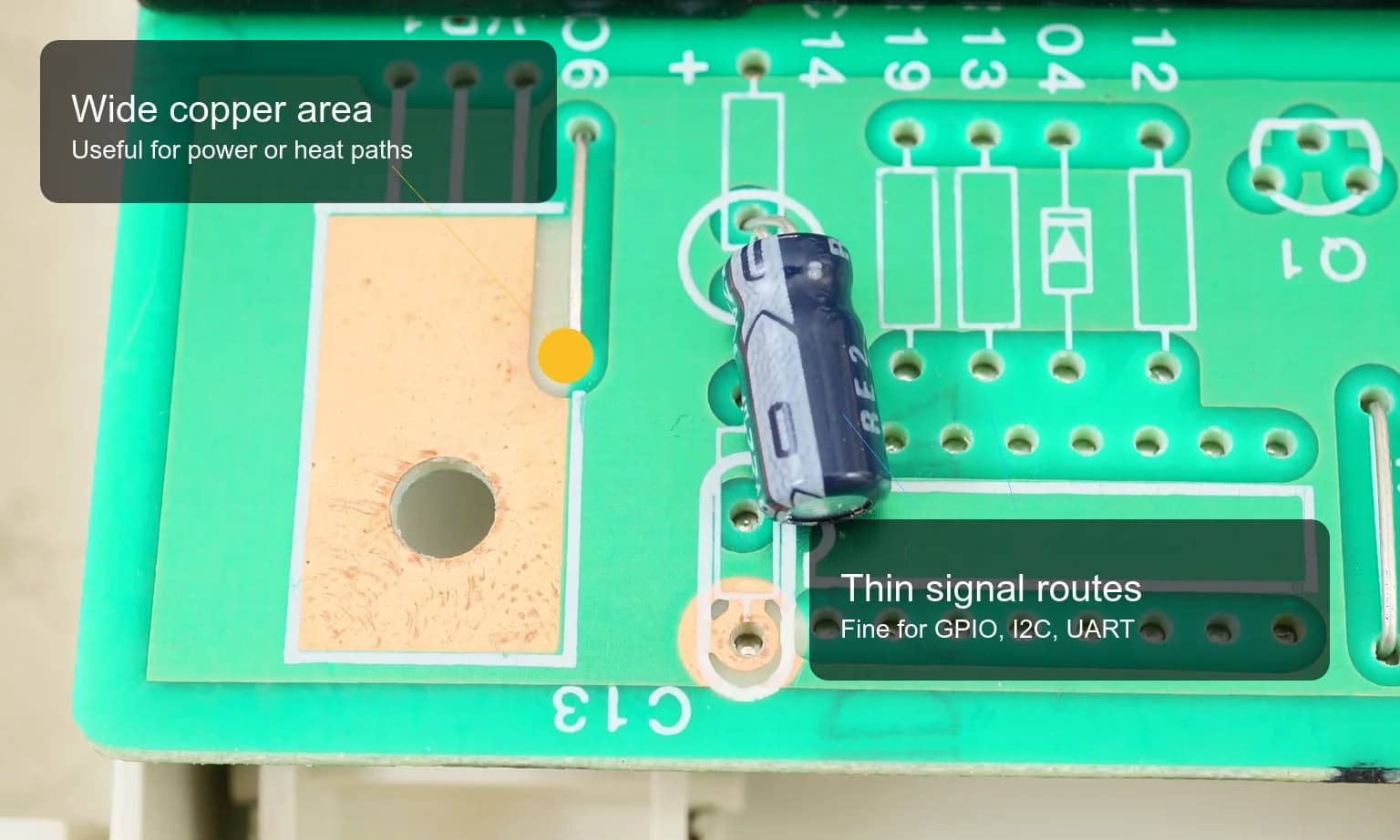
Net Classes and Trace Width: When Should a PCB Trace Be Wider?
A practical guide to PCB net classes and trace width for small boards: signal traces, 3V3, 5V, battery paths, ground, power vias, and a pre-Gerber checklist.
Read more
Resources
Tools
View all toolsTags
Everything tagged “Power Design” across notes, resources, and Mochi logs.
A practical guide to PCB net classes and trace width for small boards: signal traces, 3V3, 5V, battery paths, ground, power vias, and a pre-Gerber checklist.
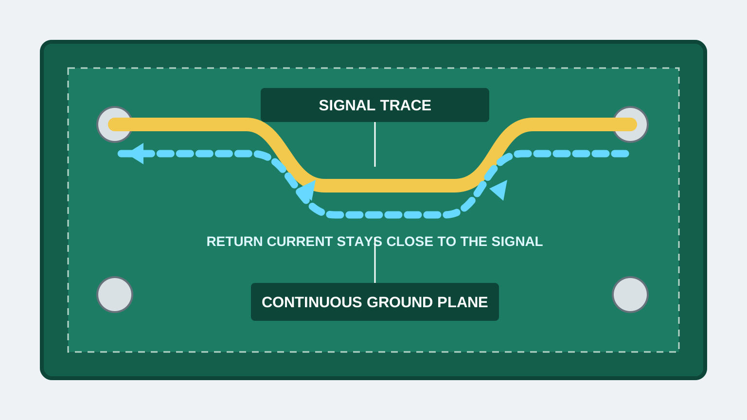
A practical guide to PCB ground planes, return current, GND layout mistakes, stitching vias, decoupling paths, and copper pour checks.
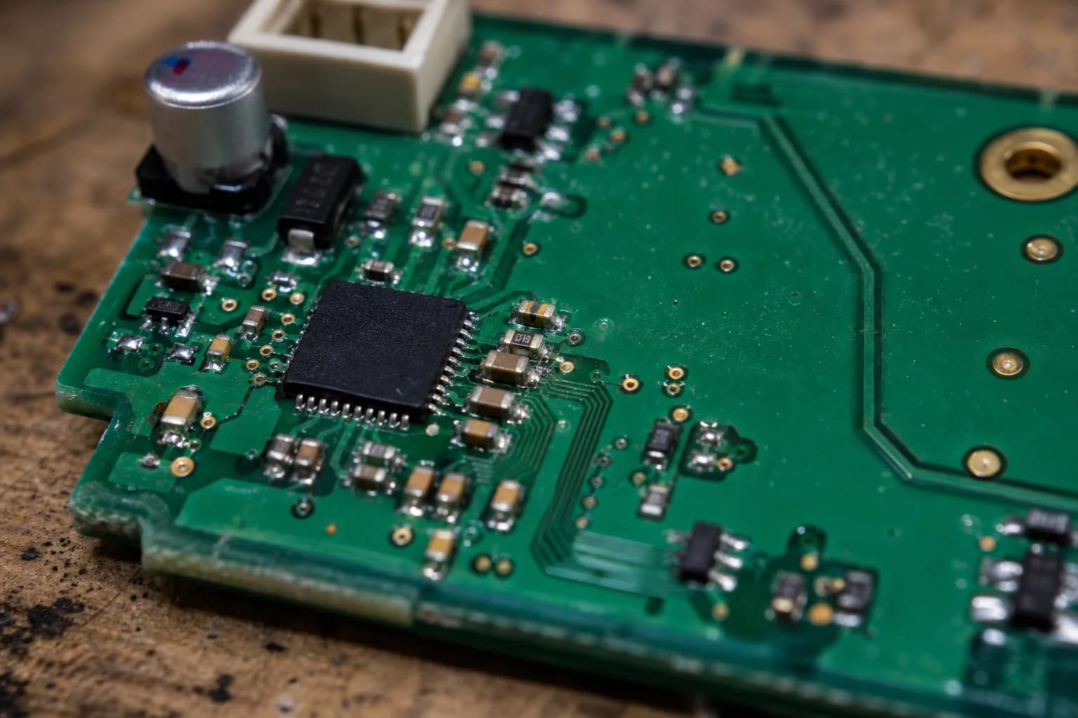
A beginner guide to choosing capacitors for circuits: capacitance, voltage rating, decoupling, ceramic types, DC bias, and ESP32 values.
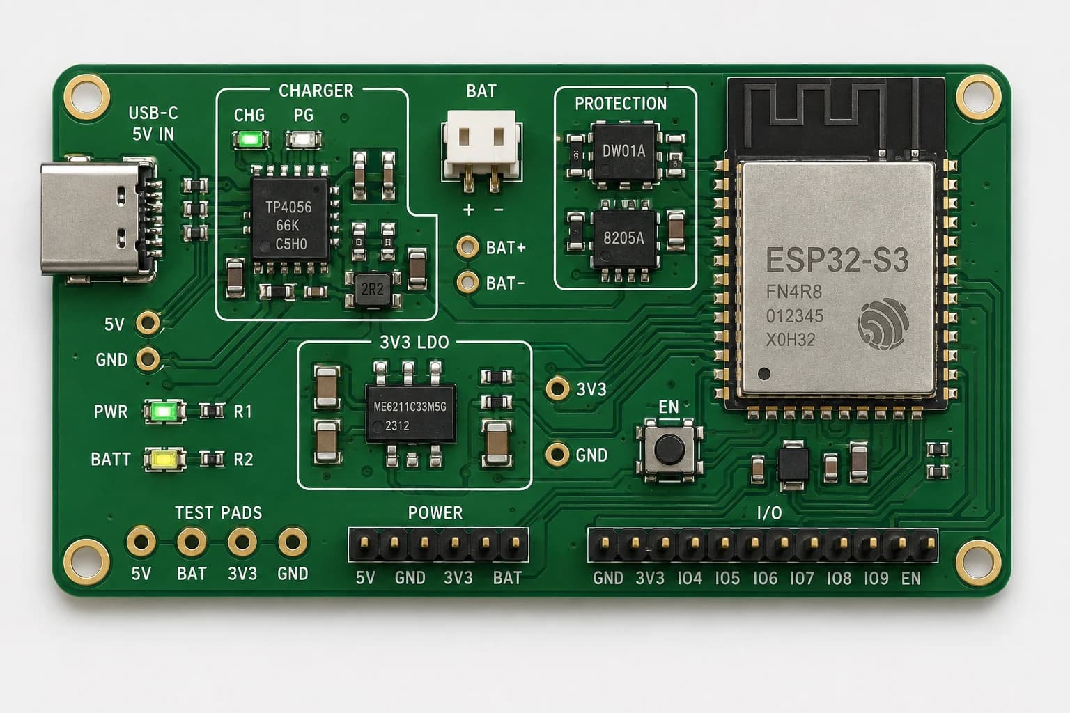
Review an ESP32-S3 battery power path from USB-C and TP4056 charging to protection, load sharing, 3.3V regulation, and load budget.
Nastrotek uses cookies for analytics and ad personalization to help us understand how the site is used. You can accept or decline non-essential cookies.