

NotesPCB Design
Net Classes and Trace Width: When Should a PCB Trace Be Wider?
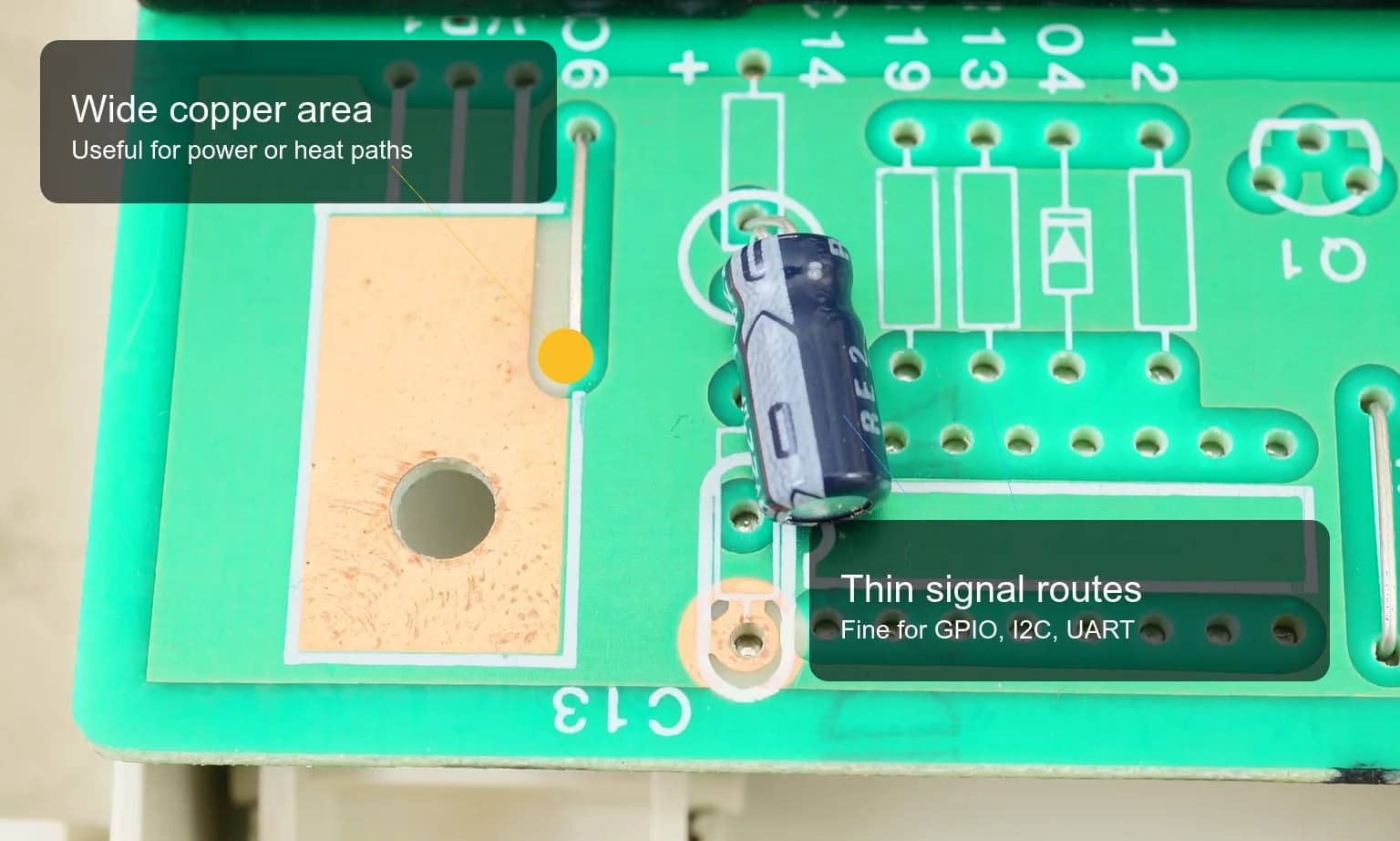
A practical guide to PCB net classes and trace width for small boards: signal traces, 3V3, 5V, battery paths, ground, power vias, and a pre-Gerber checklist.
Read more
Resources
Tools
View all toolsTags
Everything tagged “KiCad” across notes, resources, and Mochi logs.
A practical guide to PCB net classes and trace width for small boards: signal traces, 3V3, 5V, battery paths, ground, power vias, and a pre-Gerber checklist.
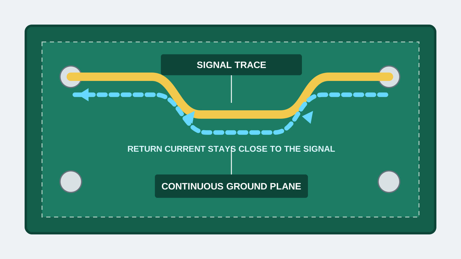
A practical guide to PCB ground planes, return current, GND layout mistakes, stitching vias, decoupling paths, and copper pour checks.

A practical PCB review checklist before fabrication: schematic, ERC, footprints, clearance, power, antenna, USB pairs, silkscreen, Gerbers, and BOM.
Nastrotek uses cookies for analytics and ad personalization to help us understand how the site is used. You can accept or decline non-essential cookies.