

Patternflow - Open-Source ESP32-S3 LED Synthesizer PCB
Author: SeungHun Lee (engmung)
Open-source Patternflow ESP32-S3 PCB for HUB75 LED matrix control, four rotary encoders, and real-time generative light patterns.
Main components
Share
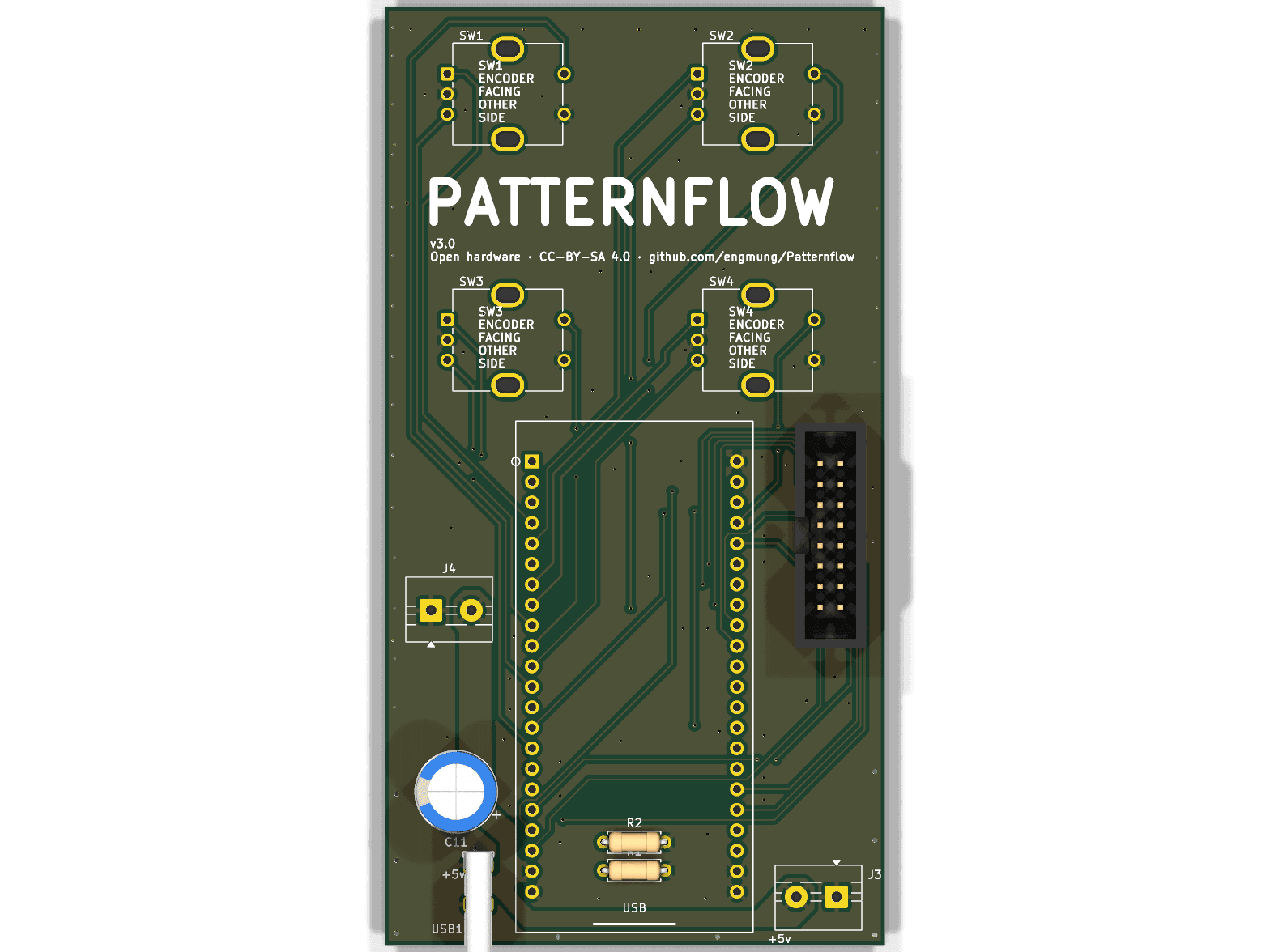
PCB photos
Quick Specs
- Main IC
- ESP32-S3-WROOM-1 N16R8 (16MB flash / 8MB PSRAM)
- Status
- Concept
What it is
An open-source controller board for a hand-played LED synthesizer: an ESP32-S3 drives a 128x64 HUB75 RGB LED matrix while four rotary encoders reshape generative light patterns live. The board is designed to be built with the ESP32-S3 DevKit socketed rather than soldered directly, so the microcontroller module itself is replaceable.
Main components
- ESP32-S3-WROOM-1 N16R8 (16MB flash, 8MB PSRAM), mounted on female headers, never soldered directly
- 4x EC11 rotary encoders with push-switch, inserted from the back of the board
- 2x8 box header carrying the HUB75 ribbon to the LED panel
- Hybrid power input: USB-C (needs CC pull-down resistors) or a 2-pin screw terminal as a solder-free bypass
- 1000µF bulk capacitor for the boot transient
What you can use it for
- Building the official Patternflow LED synthesizer from scratch
- Any project that needs an ESP32-S3 driving a HUB75 matrix with physical knob input
- A reference design for combining rotary encoders, LED matrix output, and hybrid USB-C/screw-terminal power on one board
Notes before use
- Nastrotek has not independently fabricated or tested this board yet.
- The upstream project reports its current v3.0 revision as fabricated, assembled, and verified by the original designer, including both power input options.
- Review the schematic, BOM, and license before manufacturing.
- The Type-C power path needs the R1/R2 CC pull-down resistors soldered; the source project notes those through-hole pads are fiddly to hand-solder — see issue #114 for details. The screw-terminal path avoids that entirely.
- Encoders mount on the back of the board (silkscreen marks "encoder facing other side").
- Firmware, build guide, and 3D-printed enclosure files live in the same repository if you want the complete build, not just the PCB.
Source / reference
Original hardware design by SeungHun Lee (engmung).
The firmware and web app use MIT; the hardware, designs, documentation, bundled patterns, and images shown here use CC BY-SA 4.0. Images are attributed to SeungHun Lee, and any adaptations remain under the same license. “Patternflow” identifies the original project; this page is independent and is not endorsed by it.
How to evaluate this board
Read this resource as a starting point for review, not as a board you should manufacture blindly. Open the schematic first and identify the power input, regulator path, MCU or main controller, external connectors, programming interface, and any sensor or display interfaces. Once the functional blocks are clear, it becomes much easier to decide whether the design matches your project.
For Patternflow, I would spend extra time on the LED power path, connector orientation, USB-C power entry, ESP32-S3 programming access, and any rail that feeds many LEDs at once. LED boards can look fine in the schematic and still suffer from voltage drop, heat, or awkward service access once they are installed.
Before reusing the files
- Check the license and original author notes.
- Confirm voltage levels before connecting external modules.
- Verify connector pinout against your cables and sensors.
- Review BOM availability before ordering PCBs.
- Export fresh Gerbers from the design tool if you modify anything.
- Treat untested designs as references until you have fabricated and measured them.
Good use cases
This kind of resource is useful when you want to study a real open-source hardware design, borrow part of a circuit, or compare layout decisions before creating your own board. Even if you do not fabricate the PCB directly, the schematic can still be valuable as a reference for power design, connector planning, enclosure constraints, or firmware bring-up.
For a small product prototype, the best workflow is to reuse ideas carefully: copy the principle, not the entire board without context. Mark what you changed, keep notes on assumptions, and add measurement points so the first fabricated board can teach you something useful.
Related reading
Download Resource
File details & download
- File type
- Design File
- Version
- Not specified
- File size
- Not specified
- Author
- SeungHun Lee (engmung)
- Original source
- Open original source · github.com
- License
- Not verified
- Commercial use
- Not verified
- Last checked / updated
- Jul 31, 2026
- Tested by Nastrotek
- Not verified
The license has not been verified. Do not assume this resource is free to reuse, redistribute, or use commercially.
Share
Keep exploring
Read next
Related articles
Net Classes and Trace Width: When Should a PCB Trace Be Wider?
A practical guide to PCB net classes and trace width for small boards: signal traces, 3V3, 5V, battery paths, ground, power vias, and a pre-Gerber checklist.
PCB Ground Planes: GND Is More Than a Net Name
A practical guide to PCB ground planes, return current, GND layout mistakes, stitching vias, decoupling paths, and copper pour checks.
Choosing Capacitors for Electronics: Simple Part, Easy Mistake
A beginner guide to choosing capacitors for circuits: capacitance, voltage rating, decoupling, ceramic types, DC bias, and ESP32 values.