

ESP32 Bit Pirate Dock - Voltage-Translating Carrier Board for the ESP32-S3 DevKit
Author: AndreiVladescu
Open-source ESP32 Bit Pirate Dock carrier PCB for ESP32-S3-DevKitC-1 with selectable 1.8V, 3.3V, and 5V I/O translation.
Main components
Share
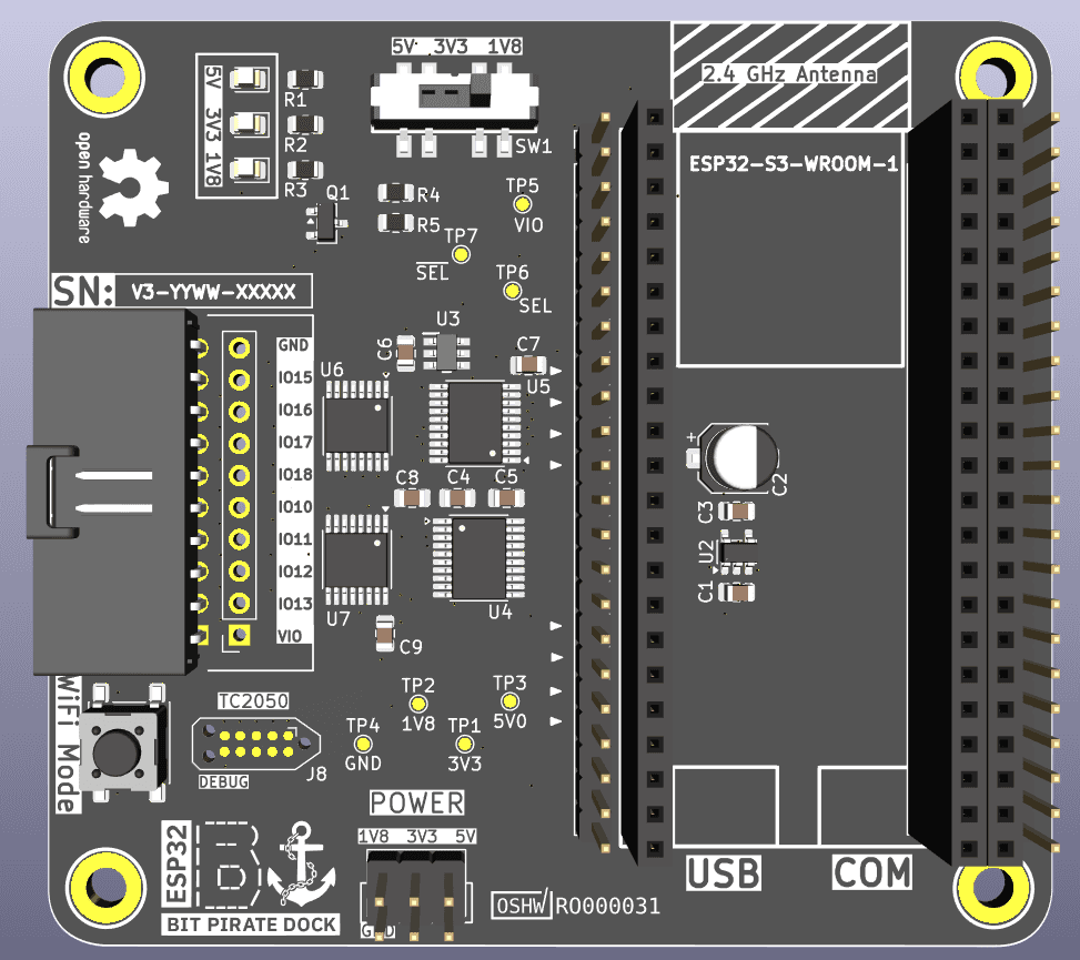
PCB photos
Quick Specs
- Main IC
- 2x TXS0108E 8-bit bidirectional level shifter
- Status
- Concept
What it is
An open-source carrier board that seats a genuine or compatible ESP32-S3-DevKitC-1 and adds selectable level/voltage translation (1.8V, 3.3V, or 5V) between the 3.3V ESP32-S3 and external peripherals. It's designed as the hardware companion to the ESP32-Bit-Pirate firmware by geo-tp, a multi-protocol hacking tool inspired by the Bus Pirate.
Main components
- 2x TXS0108E 8-bit bidirectional level shifters
- 2x TMUX1574 analog multiplexers
- TS5A3157 analog switch
- TLV75518 LDO regulator
- Voltage-select header/switch for 1.8V / 3.3V / 5V I/O
- TC2050 debug connector, WiFi-mode button, and USB/COM headers exposed from the seated DevKit
What you can use it for
- Building the official ESP32 Bit Pirate hardware to run the ESP32-Bit-Pirate firmware
- Any project that needs a socketed ESP32-S3-DevKitC-1 with selectable I/O voltage translation
- A reference design for combining bidirectional level shifting with an analog mux/switch front-end on a carrier board
Notes before use
- Nastrotek has not independently fabricated or tested this board yet.
- Requires an ESP32-S3-DevKitC-1 (genuine or a pin/dimension-compatible clone) to be procured separately — it is not part of this design.
- Only connect external peripherals at the selected translation voltage; connecting at a different voltage level can damage the ESP32 or the dock.
- Always confirm the selected I/O voltage before powering up connected hardware.
- Third-party DevKit clones work as long as header pin layout and board dimensions match the official devkit — some clones are 2.54mm wider, so measure before assuming a fit.
- Hardware design files are licensed CERN-OHL-W-2.0; documentation and images are CC BY 4.0 unless otherwise noted.
Source / reference
Original hardware design by AndreiVladescu, designed to pair with ESP32-Bit-Pirate by geo-tp.
Hardware files use CERN-OHL-W-2.0. Images and documentation on this page are attributed to AndreiVladescu under CC BY 4.0. Nastrotek is not officially affiliated with either project.
How to evaluate this board
Read this resource as a starting point for review, not as a board you should manufacture blindly. Open the schematic first and identify the power input, regulator path, MCU or main controller, external connectors, programming interface, and any sensor or display interfaces. Once the functional blocks are clear, it becomes much easier to decide whether the design matches your project.
For a dock/carrier board, I would review the pin mapping against the exact ESP32-S3 DevKit, then check level-shifter direction, connector labeling, boot/reset access, and whether the USB port remains reachable once the dock is mounted. A silkscreen mistake on a tool like this can cost more time than a schematic mistake because you use it while debugging other boards.
Before reusing the files
- Check the license and original author notes.
- Confirm voltage levels before connecting external modules.
- Verify connector pinout against your cables and sensors.
- Review BOM availability before ordering PCBs.
- Export fresh Gerbers from the design tool if you modify anything.
- Treat untested designs as references until you have fabricated and measured them.
Good use cases
This kind of resource is useful when you want to study a real open-source hardware design, borrow part of a circuit, or compare layout decisions before creating your own board. Even if you do not fabricate the PCB directly, the schematic can still be valuable as a reference for power design, connector planning, enclosure constraints, or firmware bring-up.
For a small product prototype, the best workflow is to reuse ideas carefully: copy the principle, not the entire board without context. Mark what you changed, keep notes on assumptions, and add measurement points so the first fabricated board can teach you something useful.
Related reading
Download Resource
File details & download
- File type
- Design File
- Version
- Not specified
- File size
- Not specified
- Author
- AndreiVladescu
- Original source
- Open original source · github.com
- License
- Not verified
- Commercial use
- Not verified
- Last checked / updated
- Jul 31, 2026
- Tested by Nastrotek
- Not verified
The license has not been verified. Do not assume this resource is free to reuse, redistribute, or use commercially.
Share
Keep exploring
Read next
Related articles
Net Classes and Trace Width: When Should a PCB Trace Be Wider?
A practical guide to PCB net classes and trace width for small boards: signal traces, 3V3, 5V, battery paths, ground, power vias, and a pre-Gerber checklist.
PCB Ground Planes: GND Is More Than a Net Name
A practical guide to PCB ground planes, return current, GND layout mistakes, stitching vias, decoupling paths, and copper pour checks.
Choosing Capacitors for Electronics: Simple Part, Easy Mistake
A beginner guide to choosing capacitors for circuits: capacitance, voltage rating, decoupling, ceramic types, DC bias, and ESP32 values.