

PCB Design
Net Classes and Trace Width: When Should a PCB Trace Be Wider?
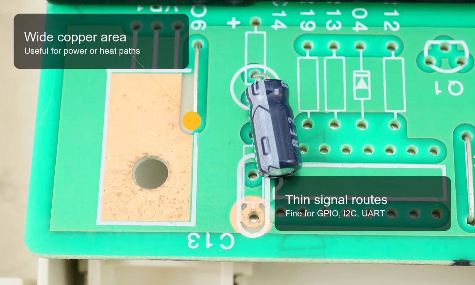
A practical guide to PCB net classes and trace width for small boards: signal traces, 3V3, 5V, battery paths, ground, power vias, and a pre-Gerber checklist.
Resources
Tools
View all toolsNotes
A practical guide to PCB net classes and trace width for small boards: signal traces, 3V3, 5V, battery paths, ground, power vias, and a pre-Gerber checklist.
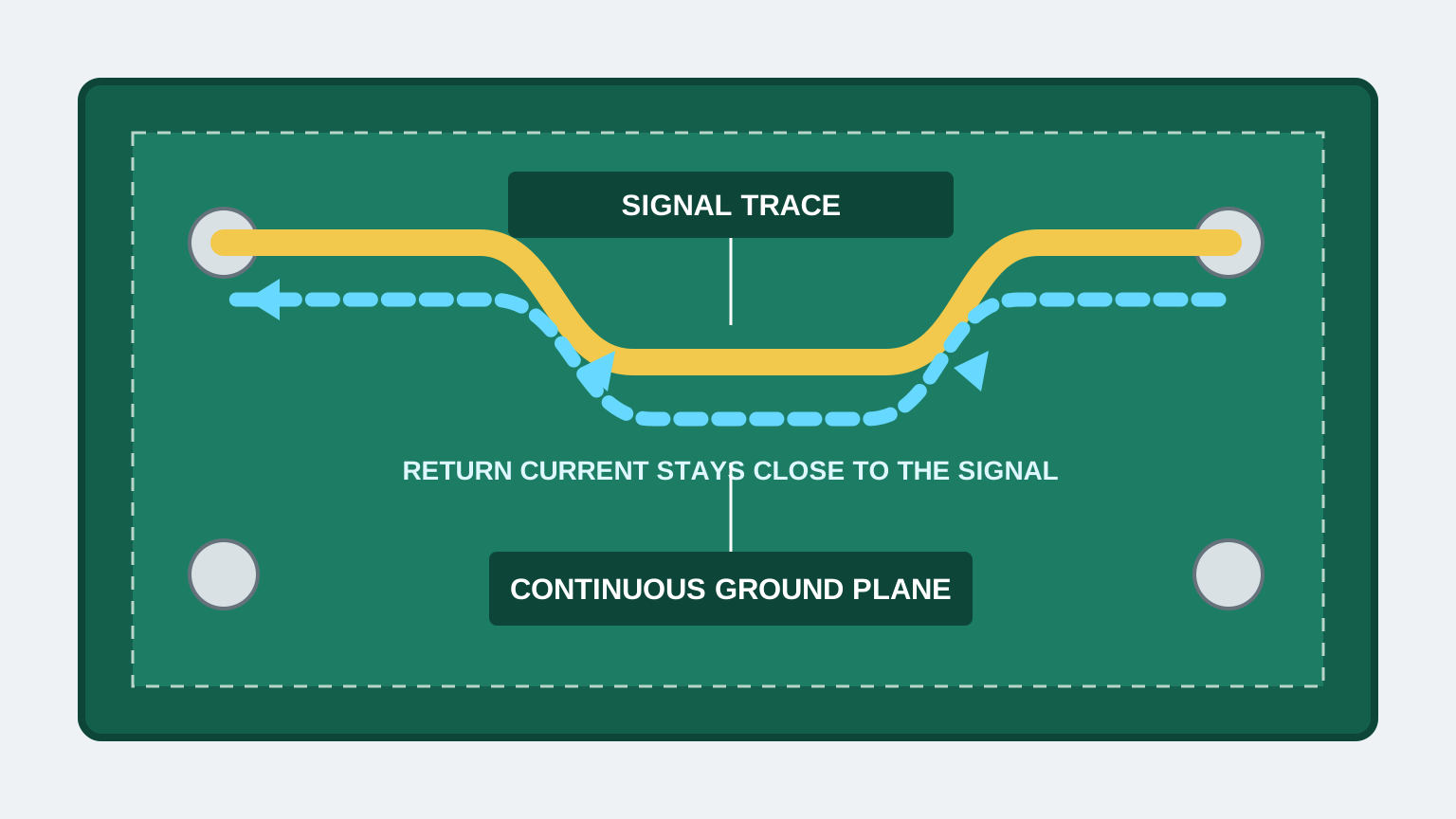
A practical guide to PCB ground planes, return current, GND layout mistakes, stitching vias, decoupling paths, and copper pour checks.
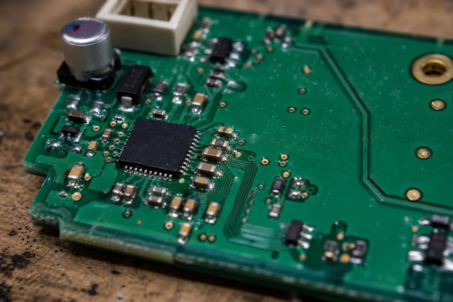
A beginner guide to choosing capacitors for circuits: capacitance, voltage rating, decoupling, ceramic types, DC bias, and ESP32 values.
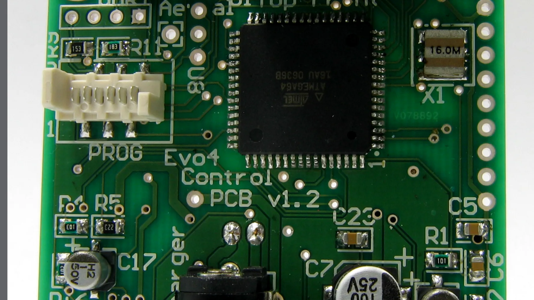
A beginner-friendly SMD soldering guide covering tools, easy parts, resistors, capacitors, multi-pin ICs, flux, hot air, and PCB inspection.
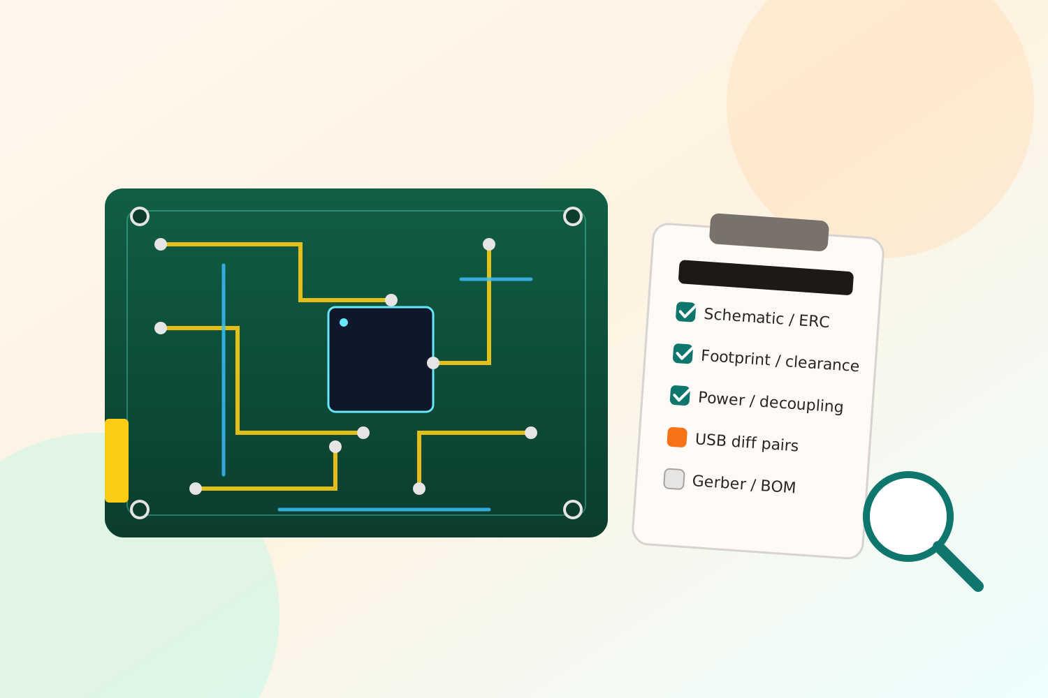
A practical PCB review checklist before fabrication: schematic, ERC, footprints, clearance, power, antenna, USB pairs, silkscreen, Gerbers, and BOM.
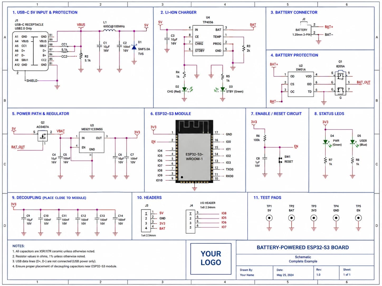
An ESP32 TouchDown case study for reviewing an open-source schematic before reuse, covering power, reset, boot, USB, connectors, and tests.
Nastrotek uses cookies for analytics and ad personalization to help us understand how the site is used. You can accept or decline non-essential cookies.